

Global Plasma Process Monitor for Semiconductor Market 2024 by Manufacturers, Regions, Type and Application, Forecast to 2030
Page: 94
Published Date: 03 Jan 2024
Category: Electronics & Semiconductor
PDF Download
Get FREE Sample
Customize Request
-
 Description
 Table of Contents
 Table of Figures
 Research Methodology
 Companies Mentioned
 Related Reports
 Product Tags

 Table of Contents
 Table of Figures
 Research Methodology
 Companies Mentioned
 Related Reports
 Product Tags

Description
According to our (Global Info Research) latest study, the global Plasma Process Monitor for Semiconductor market size was valued at USD million in 2023 and is forecast to a readjusted size of USD million by 2030 with a CAGR of % during review period.

Plasma monitors are used to monitor plasma emissions during the semiconductor manufacturing process, for example, etching and sputtering.

The global market for semiconductor was estimated at US$ 579 billion in the year 2022, is projected to US$ 790 billion by 2029, growing at a CAGR of 6% during the forecast period. Although some major categories are still double-digit year-over-year growth in 2022, led by Analog with 20.76%, Sensor with 16.31%, and Logic with 14.46% growth, Memory declined with 12.64% year over year. The microprocessor (MPU) and microcontroller (MCU) segments will experience stagnant growth due to weak shipments and investment in notebooks, computers, and standard desktops. In the current market scenario, the growing popularity of IoT-based electronics is stimulating the need for powerful processors and controllers. Hybrid MPUs and MCUs provide real-time embedded processing and control for the topmost IoT-based applications, resulting in significant market growth. The Analog IC segment is expected to grow gradually, while demand from the networking and communications industries is limited. Few of the emerging trends in the growing demand for Analog integrated circuits include signal conversion, automotive-specific Analog applications, and power management. They drive the growing demand for discrete power devices.

The Global Info Research report includes an overview of the development of the Plasma Process Monitor for Semiconductor industry chain, the market status of Etching (200 nm-500 nm, 500 nm-950 nm), Spattering (200 nm-500 nm, 500 nm-950 nm), and key enterprises in developed and developing market, and analysed the cutting-edge technology, patent, hot applications and market trends of Plasma Process Monitor for Semiconductor.

Regionally, the report analyzes the Plasma Process Monitor for Semiconductor markets in key regions. North America and Europe are experiencing steady growth, driven by government initiatives and increasing consumer awareness. Asia-Pacific, particularly China, leads the global Plasma Process Monitor for Semiconductor market, with robust domestic demand, supportive policies, and a strong manufacturing base.

Key Features:
The report presents comprehensive understanding of the Plasma Process Monitor for Semiconductor market. It provides a holistic view of the industry, as well as detailed insights into individual components and stakeholders. The report analysis market dynamics, trends, challenges, and opportunities within the Plasma Process Monitor for Semiconductor industry.

The report involves analyzing the market at a macro level:
Market Sizing and Segmentation: Report collect data on the overall market size, including the sales quantity (Units), revenue generated, and market share of different by Type (e.g., 200 nm-500 nm, 500 nm-950 nm).

Industry Analysis: Report analyse the broader industry trends, such as government policies and regulations, technological advancements, consumer preferences, and market dynamics. This analysis helps in understanding the key drivers and challenges influencing the Plasma Process Monitor for Semiconductor market.

Regional Analysis: The report involves examining the Plasma Process Monitor for Semiconductor market at a regional or national level. Report analyses regional factors such as government incentives, infrastructure development, economic conditions, and consumer behaviour to identify variations and opportunities within different markets.

Market Projections: Report covers the gathered data and analysis to make future projections and forecasts for the Plasma Process Monitor for Semiconductor market. This may include estimating market growth rates, predicting market demand, and identifying emerging trends.

The report also involves a more granular approach to Plasma Process Monitor for Semiconductor:
Company Analysis: Report covers individual Plasma Process Monitor for Semiconductor manufacturers, suppliers, and other relevant industry players. This analysis includes studying their financial performance, market positioning, product portfolios, partnerships, and strategies.

Consumer Analysis: Report covers data on consumer behaviour, preferences, and attitudes towards Plasma Process Monitor for Semiconductor This may involve surveys, interviews, and analysis of consumer reviews and feedback from different by Application (Etching, Spattering).

Technology Analysis: Report covers specific technologies relevant to Plasma Process Monitor for Semiconductor. It assesses the current state, advancements, and potential future developments in Plasma Process Monitor for Semiconductor areas.

Competitive Landscape: By analyzing individual companies, suppliers, and consumers, the report present insights into the competitive landscape of the Plasma Process Monitor for Semiconductor market. This analysis helps understand market share, competitive advantages, and potential areas for differentiation among industry players.

Market Validation: The report involves validating findings and projections through primary research, such as surveys, interviews, and focus groups.

Market Segmentation
Plasma Process Monitor for Semiconductor market is split by Type and by Application. For the period 2019-2030, the growth among segments provides accurate calculations and forecasts for consumption value by Type, and by Application in terms of volume and value.

Market segment by Type
    200 nm-500 nm
    500 nm-950 nm

Market segment by Application
    Etching
    Spattering
    CVD

Major players covered
    Hamamatsu Photonics
    HORIBA
    PLASUS
    Extrel
    Plasmetrex GmbH

Market segment by region, regional analysis covers
    North America (United States, Canada and Mexico)
    Europe (Germany, France, United Kingdom, Russia, Italy, and Rest of Europe)
    Asia-Pacific (China, Japan, Korea, India, Southeast Asia, and Australia)
    South America (Brazil, Argentina, Colombia, and Rest of South America)
    Middle East & Africa (Saudi Arabia, UAE, Egypt, South Africa, and Rest of Middle East & Africa)

The content of the study subjects, includes a total of 15 chapters:
Chapter 1, to describe Plasma Process Monitor for Semiconductor product scope, market overview, market estimation caveats and base year.
Chapter 2, to profile the top manufacturers of Plasma Process Monitor for Semiconductor, with price, sales, revenue and global market share of Plasma Process Monitor for Semiconductor from 2019 to 2024.
Chapter 3, the Plasma Process Monitor for Semiconductor competitive situation, sales quantity, revenue and global market share of top manufacturers are analyzed emphatically by landscape contrast.
Chapter 4, the Plasma Process Monitor for Semiconductor breakdown data are shown at the regional level, to show the sales quantity, consumption value and growth by regions, from 2019 to 2030.
Chapter 5 and 6, to segment the sales by Type and application, with sales market share and growth rate by type, application, from 2019 to 2030.
Chapter 7, 8, 9, 10 and 11, to break the sales data at the country level, with sales quantity, consumption value and market share for key countries in the world, from 2017 to 2023.and Plasma Process Monitor for Semiconductor market forecast, by regions, type and application, with sales and revenue, from 2025 to 2030.
Chapter 12, market dynamics, drivers, restraints, trends and Porters Five Forces analysis.
Chapter 13, the key raw materials and key suppliers, and industry chain of Plasma Process Monitor for Semiconductor.
Chapter 14 and 15, to describe Plasma Process Monitor for Semiconductor sales channel, distributors, customers, research findings and conclusion.
Table of Contents
1 Market Overview
1.1 Product Overview and Scope of Plasma Process Monitor for Semiconductor
1.2 Market Estimation Caveats and Base Year
1.3 Market Analysis by Type
1.3.1 Overview: Global Plasma Process Monitor for Semiconductor Consumption Value by Type: 2019 Versus 2023 Versus 2030
1.3.2 200 nm-500 nm
1.3.3 500 nm-950 nm
1.4 Market Analysis by Application
1.4.1 Overview: Global Plasma Process Monitor for Semiconductor Consumption Value by Application: 2019 Versus 2023 Versus 2030
1.4.2 Etching
1.4.3 Spattering
1.4.4 CVD
1.5 Global Plasma Process Monitor for Semiconductor Market Size & Forecast
1.5.1 Global Plasma Process Monitor for Semiconductor Consumption Value (2019 & 2023 & 2030)
1.5.2 Global Plasma Process Monitor for Semiconductor Sales Quantity (2019-2030)
1.5.3 Global Plasma Process Monitor for Semiconductor Average Price (2019-2030)
2.1 Hamamatsu Photonics
2.1.1 Hamamatsu Photonics Details
2.1.2 Hamamatsu Photonics Major Business
2.1.3 Hamamatsu Photonics Plasma Process Monitor for Semiconductor Product and Services
2.1.4 Hamamatsu Photonics Plasma Process Monitor for Semiconductor Sales Quantity, Average Price, Revenue, Gross Margin and Market Share (2019-2024)
2.1.5 Hamamatsu Photonics Recent Developments/Updates
2.2 HORIBA
2.2.1 HORIBA Details
2.2.2 HORIBA Major Business
2.2.3 HORIBA Plasma Process Monitor for Semiconductor Product and Services
2.2.4 HORIBA Plasma Process Monitor for Semiconductor Sales Quantity, Average Price, Revenue, Gross Margin and Market Share (2019-2024)
2.2.5 HORIBA Recent Developments/Updates
2.3 PLASUS
2.3.1 PLASUS Details
2.3.2 PLASUS Major Business
2.3.3 PLASUS Plasma Process Monitor for Semiconductor Product and Services
2.3.4 PLASUS Plasma Process Monitor for Semiconductor Sales Quantity, Average Price, Revenue, Gross Margin and Market Share (2019-2024)
2.3.5 PLASUS Recent Developments/Updates
2.4 Extrel
2.4.1 Extrel Details
2.4.2 Extrel Major Business
2.4.3 Extrel Plasma Process Monitor for Semiconductor Product and Services
2.4.4 Extrel Plasma Process Monitor for Semiconductor Sales Quantity, Average Price, Revenue, Gross Margin and Market Share (2019-2024)
2.4.5 Extrel Recent Developments/Updates
2.5 Plasmetrex GmbH
2.5.1 Plasmetrex GmbH Details
2.5.2 Plasmetrex GmbH Major Business
2.5.3 Plasmetrex GmbH Plasma Process Monitor for Semiconductor Product and Services
2.5.4 Plasmetrex GmbH Plasma Process Monitor for Semiconductor Sales Quantity, Average Price, Revenue, Gross Margin and Market Share (2019-2024)
2.5.5 Plasmetrex GmbH Recent Developments/Updates
3.1 Global Plasma Process Monitor for Semiconductor Sales Quantity by Manufacturer (2019-2024)
3.2 Global Plasma Process Monitor for Semiconductor Revenue by Manufacturer (2019-2024)
3.3 Global Plasma Process Monitor for Semiconductor Average Price by Manufacturer (2019-2024)
3.4 Market Share Analysis (2023)
3.4.1 Producer Shipments of Plasma Process Monitor for Semiconductor by Manufacturer Revenue ($MM) and Market Share (%): 2023
3.4.2 Top 3 Plasma Process Monitor for Semiconductor Manufacturer Market Share in 2023
3.4.2 Top 6 Plasma Process Monitor for Semiconductor Manufacturer Market Share in 2023
3.5 Plasma Process Monitor for Semiconductor Market: Overall Company Footprint Analysis
3.5.1 Plasma Process Monitor for Semiconductor Market: Region Footprint
3.5.2 Plasma Process Monitor for Semiconductor Market: Company Product Type Footprint
3.5.3 Plasma Process Monitor for Semiconductor Market: Company Product Application Footprint
3.6 New Market Entrants and Barriers to Market Entry
3.7 Mergers, Acquisition, Agreements, and Collaborations
4.1 Global Plasma Process Monitor for Semiconductor Market Size by Region
4.1.1 Global Plasma Process Monitor for Semiconductor Sales Quantity by Region (2019-2030)
4.1.2 Global Plasma Process Monitor for Semiconductor Consumption Value by Region (2019-2030)
4.1.3 Global Plasma Process Monitor for Semiconductor Average Price by Region (2019-2030)
4.2 North America Plasma Process Monitor for Semiconductor Consumption Value (2019-2030)
4.3 Europe Plasma Process Monitor for Semiconductor Consumption Value (2019-2030)
4.4 Asia-Pacific Plasma Process Monitor for Semiconductor Consumption Value (2019-2030)
4.5 South America Plasma Process Monitor for Semiconductor Consumption Value (2019-2030)
4.6 Middle East and Africa Plasma Process Monitor for Semiconductor Consumption Value (2019-2030)
5.1 Global Plasma Process Monitor for Semiconductor Sales Quantity by Type (2019-2030)
5.2 Global Plasma Process Monitor for Semiconductor Consumption Value by Type (2019-2030)
5.3 Global Plasma Process Monitor for Semiconductor Average Price by Type (2019-2030)
6.1 Global Plasma Process Monitor for Semiconductor Sales Quantity by Application (2019-2030)
6.2 Global Plasma Process Monitor for Semiconductor Consumption Value by Application (2019-2030)
6.3 Global Plasma Process Monitor for Semiconductor Average Price by Application (2019-2030)
7.1 North America Plasma Process Monitor for Semiconductor Sales Quantity by Type (2019-2030)
7.2 North America Plasma Process Monitor for Semiconductor Sales Quantity by Application (2019-2030)
7.3 North America Plasma Process Monitor for Semiconductor Market Size by Country
7.3.1 North America Plasma Process Monitor for Semiconductor Sales Quantity by Country (2019-2030)
7.3.2 North America Plasma Process Monitor for Semiconductor Consumption Value by Country (2019-2030)
7.3.3 United States Market Size and Forecast (2019-2030)
7.3.4 Canada Market Size and Forecast (2019-2030)
7.3.5 Mexico Market Size and Forecast (2019-2030)
8.1 Europe Plasma Process Monitor for Semiconductor Sales Quantity by Type (2019-2030)
8.2 Europe Plasma Process Monitor for Semiconductor Sales Quantity by Application (2019-2030)
8.3 Europe Plasma Process Monitor for Semiconductor Market Size by Country
8.3.1 Europe Plasma Process Monitor for Semiconductor Sales Quantity by Country (2019-2030)
8.3.2 Europe Plasma Process Monitor for Semiconductor Consumption Value by Country (2019-2030)
8.3.3 Germany Market Size and Forecast (2019-2030)
8.3.4 France Market Size and Forecast (2019-2030)
8.3.5 United Kingdom Market Size and Forecast (2019-2030)
8.3.6 Russia Market Size and Forecast (2019-2030)
8.3.7 Italy Market Size and Forecast (2019-2030)
9.1 Asia-Pacific Plasma Process Monitor for Semiconductor Sales Quantity by Type (2019-2030)
9.2 Asia-Pacific Plasma Process Monitor for Semiconductor Sales Quantity by Application (2019-2030)
9.3 Asia-Pacific Plasma Process Monitor for Semiconductor Market Size by Region
9.3.1 Asia-Pacific Plasma Process Monitor for Semiconductor Sales Quantity by Region (2019-2030)
9.3.2 Asia-Pacific Plasma Process Monitor for Semiconductor Consumption Value by Region (2019-2030)
9.3.3 China Market Size and Forecast (2019-2030)
9.3.4 Japan Market Size and Forecast (2019-2030)
9.3.5 Korea Market Size and Forecast (2019-2030)
9.3.6 India Market Size and Forecast (2019-2030)
9.3.7 Southeast Asia Market Size and Forecast (2019-2030)
9.3.8 Australia Market Size and Forecast (2019-2030)
10.1 South America Plasma Process Monitor for Semiconductor Sales Quantity by Type (2019-2030)
10.2 South America Plasma Process Monitor for Semiconductor Sales Quantity by Application (2019-2030)
10.3 South America Plasma Process Monitor for Semiconductor Market Size by Country
10.3.1 South America Plasma Process Monitor for Semiconductor Sales Quantity by Country (2019-2030)
10.3.2 South America Plasma Process Monitor for Semiconductor Consumption Value by Country (2019-2030)
10.3.3 Brazil Market Size and Forecast (2019-2030)
10.3.4 Argentina Market Size and Forecast (2019-2030)
11.1 Middle East & Africa Plasma Process Monitor for Semiconductor Sales Quantity by Type (2019-2030)
11.2 Middle East & Africa Plasma Process Monitor for Semiconductor Sales Quantity by Application (2019-2030)
11.3 Middle East & Africa Plasma Process Monitor for Semiconductor Market Size by Country
11.3.1 Middle East & Africa Plasma Process Monitor for Semiconductor Sales Quantity by Country (2019-2030)
11.3.2 Middle East & Africa Plasma Process Monitor for Semiconductor Consumption Value by Country (2019-2030)
11.3.3 Turkey Market Size and Forecast (2019-2030)
11.3.4 Egypt Market Size and Forecast (2019-2030)
11.3.5 Saudi Arabia Market Size and Forecast (2019-2030)
11.3.6 South Africa Market Size and Forecast (2019-2030)
12.1 Plasma Process Monitor for Semiconductor Market Drivers
12.2 Plasma Process Monitor for Semiconductor Market Restraints
12.3 Plasma Process Monitor for Semiconductor Trends Analysis
12.4 Porters Five Forces Analysis
12.4.1 Threat of New Entrants
12.4.2 Bargaining Power of Suppliers
12.4.3 Bargaining Power of Buyers
12.4.4 Threat of Substitutes
12.4.5 Competitive Rivalry
13.1 Raw Material of Plasma Process Monitor for Semiconductor and Key Manufacturers
13.2 Manufacturing Costs Percentage of Plasma Process Monitor for Semiconductor
13.3 Plasma Process Monitor for Semiconductor Production Process
13.4 Plasma Process Monitor for Semiconductor Industrial Chain
14.1 Sales Channel
14.1.1 Direct to End-User
14.1.2 Distributors
14.2 Plasma Process Monitor for Semiconductor Typical Distributors
14.3 Plasma Process Monitor for Semiconductor Typical Customers
16.1 Methodology
16.2 Research Process and Data Source
16.3 Disclaimer
Table of Figures
List of Tables
    Table 1. Global Plasma Process Monitor for Semiconductor Consumption Value by Type, (USD Million), 2019 & 2023 & 2030
    Table 2. Global Plasma Process Monitor for Semiconductor Consumption Value by Application, (USD Million), 2019 & 2023 & 2030
    Table 3. Hamamatsu Photonics Basic Information, Manufacturing Base and Competitors
    Table 4. Hamamatsu Photonics Major Business
    Table 5. Hamamatsu Photonics Plasma Process Monitor for Semiconductor Product and Services
    Table 6. Hamamatsu Photonics Plasma Process Monitor for Semiconductor Sales Quantity (Units), Average Price (US$/Unit), Revenue (USD Million), Gross Margin and Market Share (2019-2024)
    Table 7. Hamamatsu Photonics Recent Developments/Updates
    Table 8. HORIBA Basic Information, Manufacturing Base and Competitors
    Table 9. HORIBA Major Business
    Table 10. HORIBA Plasma Process Monitor for Semiconductor Product and Services
    Table 11. HORIBA Plasma Process Monitor for Semiconductor Sales Quantity (Units), Average Price (US$/Unit), Revenue (USD Million), Gross Margin and Market Share (2019-2024)
    Table 12. HORIBA Recent Developments/Updates
    Table 13. PLASUS Basic Information, Manufacturing Base and Competitors
    Table 14. PLASUS Major Business
    Table 15. PLASUS Plasma Process Monitor for Semiconductor Product and Services
    Table 16. PLASUS Plasma Process Monitor for Semiconductor Sales Quantity (Units), Average Price (US$/Unit), Revenue (USD Million), Gross Margin and Market Share (2019-2024)
    Table 17. PLASUS Recent Developments/Updates
    Table 18. Extrel Basic Information, Manufacturing Base and Competitors
    Table 19. Extrel Major Business
    Table 20. Extrel Plasma Process Monitor for Semiconductor Product and Services
    Table 21. Extrel Plasma Process Monitor for Semiconductor Sales Quantity (Units), Average Price (US$/Unit), Revenue (USD Million), Gross Margin and Market Share (2019-2024)
    Table 22. Extrel Recent Developments/Updates
    Table 23. Plasmetrex GmbH Basic Information, Manufacturing Base and Competitors
    Table 24. Plasmetrex GmbH Major Business
    Table 25. Plasmetrex GmbH Plasma Process Monitor for Semiconductor Product and Services
    Table 26. Plasmetrex GmbH Plasma Process Monitor for Semiconductor Sales Quantity (Units), Average Price (US$/Unit), Revenue (USD Million), Gross Margin and Market Share (2019-2024)
    Table 27. Plasmetrex GmbH Recent Developments/Updates
    Table 28. Global Plasma Process Monitor for Semiconductor Sales Quantity by Manufacturer (2019-2024) & (Units)
    Table 29. Global Plasma Process Monitor for Semiconductor Revenue by Manufacturer (2019-2024) & (USD Million)
    Table 30. Global Plasma Process Monitor for Semiconductor Average Price by Manufacturer (2019-2024) & (US$/Unit)
    Table 31. Market Position of Manufacturers in Plasma Process Monitor for Semiconductor, (Tier 1, Tier 2, and Tier 3), Based on Consumption Value in 2023
    Table 32. Head Office and Plasma Process Monitor for Semiconductor Production Site of Key Manufacturer
    Table 33. Plasma Process Monitor for Semiconductor Market: Company Product Type Footprint
    Table 34. Plasma Process Monitor for Semiconductor Market: Company Product Application Footprint
    Table 35. Plasma Process Monitor for Semiconductor New Market Entrants and Barriers to Market Entry
    Table 36. Plasma Process Monitor for Semiconductor Mergers, Acquisition, Agreements, and Collaborations
    Table 37. Global Plasma Process Monitor for Semiconductor Sales Quantity by Region (2019-2024) & (Units)
    Table 38. Global Plasma Process Monitor for Semiconductor Sales Quantity by Region (2025-2030) & (Units)
    Table 39. Global Plasma Process Monitor for Semiconductor Consumption Value by Region (2019-2024) & (USD Million)
    Table 40. Global Plasma Process Monitor for Semiconductor Consumption Value by Region (2025-2030) & (USD Million)
    Table 41. Global Plasma Process Monitor for Semiconductor Average Price by Region (2019-2024) & (US$/Unit)
    Table 42. Global Plasma Process Monitor for Semiconductor Average Price by Region (2025-2030) & (US$/Unit)
    Table 43. Global Plasma Process Monitor for Semiconductor Sales Quantity by Type (2019-2024) & (Units)
    Table 44. Global Plasma Process Monitor for Semiconductor Sales Quantity by Type (2025-2030) & (Units)
    Table 45. Global Plasma Process Monitor for Semiconductor Consumption Value by Type (2019-2024) & (USD Million)
    Table 46. Global Plasma Process Monitor for Semiconductor Consumption Value by Type (2025-2030) & (USD Million)
    Table 47. Global Plasma Process Monitor for Semiconductor Average Price by Type (2019-2024) & (US$/Unit)
    Table 48. Global Plasma Process Monitor for Semiconductor Average Price by Type (2025-2030) & (US$/Unit)
    Table 49. Global Plasma Process Monitor for Semiconductor Sales Quantity by Application (2019-2024) & (Units)
    Table 50. Global Plasma Process Monitor for Semiconductor Sales Quantity by Application (2025-2030) & (Units)
    Table 51. Global Plasma Process Monitor for Semiconductor Consumption Value by Application (2019-2024) & (USD Million)
    Table 52. Global Plasma Process Monitor for Semiconductor Consumption Value by Application (2025-2030) & (USD Million)
    Table 53. Global Plasma Process Monitor for Semiconductor Average Price by Application (2019-2024) & (US$/Unit)
    Table 54. Global Plasma Process Monitor for Semiconductor Average Price by Application (2025-2030) & (US$/Unit)
    Table 55. North America Plasma Process Monitor for Semiconductor Sales Quantity by Type (2019-2024) & (Units)
    Table 56. North America Plasma Process Monitor for Semiconductor Sales Quantity by Type (2025-2030) & (Units)
    Table 57. North America Plasma Process Monitor for Semiconductor Sales Quantity by Application (2019-2024) & (Units)
    Table 58. North America Plasma Process Monitor for Semiconductor Sales Quantity by Application (2025-2030) & (Units)
    Table 59. North America Plasma Process Monitor for Semiconductor Sales Quantity by Country (2019-2024) & (Units)
    Table 60. North America Plasma Process Monitor for Semiconductor Sales Quantity by Country (2025-2030) & (Units)
    Table 61. North America Plasma Process Monitor for Semiconductor Consumption Value by Country (2019-2024) & (USD Million)
    Table 62. North America Plasma Process Monitor for Semiconductor Consumption Value by Country (2025-2030) & (USD Million)
    Table 63. Europe Plasma Process Monitor for Semiconductor Sales Quantity by Type (2019-2024) & (Units)
    Table 64. Europe Plasma Process Monitor for Semiconductor Sales Quantity by Type (2025-2030) & (Units)
    Table 65. Europe Plasma Process Monitor for Semiconductor Sales Quantity by Application (2019-2024) & (Units)
    Table 66. Europe Plasma Process Monitor for Semiconductor Sales Quantity by Application (2025-2030) & (Units)
    Table 67. Europe Plasma Process Monitor for Semiconductor Sales Quantity by Country (2019-2024) & (Units)
    Table 68. Europe Plasma Process Monitor for Semiconductor Sales Quantity by Country (2025-2030) & (Units)
    Table 69. Europe Plasma Process Monitor for Semiconductor Consumption Value by Country (2019-2024) & (USD Million)
    Table 70. Europe Plasma Process Monitor for Semiconductor Consumption Value by Country (2025-2030) & (USD Million)
    Table 71. Asia-Pacific Plasma Process Monitor for Semiconductor Sales Quantity by Type (2019-2024) & (Units)
    Table 72. Asia-Pacific Plasma Process Monitor for Semiconductor Sales Quantity by Type (2025-2030) & (Units)
    Table 73. Asia-Pacific Plasma Process Monitor for Semiconductor Sales Quantity by Application (2019-2024) & (Units)
    Table 74. Asia-Pacific Plasma Process Monitor for Semiconductor Sales Quantity by Application (2025-2030) & (Units)
    Table 75. Asia-Pacific Plasma Process Monitor for Semiconductor Sales Quantity by Region (2019-2024) & (Units)
    Table 76. Asia-Pacific Plasma Process Monitor for Semiconductor Sales Quantity by Region (2025-2030) & (Units)
    Table 77. Asia-Pacific Plasma Process Monitor for Semiconductor Consumption Value by Region (2019-2024) & (USD Million)
    Table 78. Asia-Pacific Plasma Process Monitor for Semiconductor Consumption Value by Region (2025-2030) & (USD Million)
    Table 79. South America Plasma Process Monitor for Semiconductor Sales Quantity by Type (2019-2024) & (Units)
    Table 80. South America Plasma Process Monitor for Semiconductor Sales Quantity by Type (2025-2030) & (Units)
    Table 81. South America Plasma Process Monitor for Semiconductor Sales Quantity by Application (2019-2024) & (Units)
    Table 82. South America Plasma Process Monitor for Semiconductor Sales Quantity by Application (2025-2030) & (Units)
    Table 83. South America Plasma Process Monitor for Semiconductor Sales Quantity by Country (2019-2024) & (Units)
    Table 84. South America Plasma Process Monitor for Semiconductor Sales Quantity by Country (2025-2030) & (Units)
    Table 85. South America Plasma Process Monitor for Semiconductor Consumption Value by Country (2019-2024) & (USD Million)
    Table 86. South America Plasma Process Monitor for Semiconductor Consumption Value by Country (2025-2030) & (USD Million)
    Table 87. Middle East & Africa Plasma Process Monitor for Semiconductor Sales Quantity by Type (2019-2024) & (Units)
    Table 88. Middle East & Africa Plasma Process Monitor for Semiconductor Sales Quantity by Type (2025-2030) & (Units)
    Table 89. Middle East & Africa Plasma Process Monitor for Semiconductor Sales Quantity by Application (2019-2024) & (Units)
    Table 90. Middle East & Africa Plasma Process Monitor for Semiconductor Sales Quantity by Application (2025-2030) & (Units)
    Table 91. Middle East & Africa Plasma Process Monitor for Semiconductor Sales Quantity by Region (2019-2024) & (Units)
    Table 92. Middle East & Africa Plasma Process Monitor for Semiconductor Sales Quantity by Region (2025-2030) & (Units)
    Table 93. Middle East & Africa Plasma Process Monitor for Semiconductor Consumption Value by Region (2019-2024) & (USD Million)
    Table 94. Middle East & Africa Plasma Process Monitor for Semiconductor Consumption Value by Region (2025-2030) & (USD Million)
    Table 95. Plasma Process Monitor for Semiconductor Raw Material
    Table 96. Key Manufacturers of Plasma Process Monitor for Semiconductor Raw Materials
    Table 97. Plasma Process Monitor for Semiconductor Typical Distributors
    Table 98. Plasma Process Monitor for Semiconductor Typical Customers
List of Figures
    Figure 1. Plasma Process Monitor for Semiconductor Picture
    Figure 2. Global Plasma Process Monitor for Semiconductor Consumption Value by Type, (USD Million), 2019 & 2023 & 2030
    Figure 3. Global Plasma Process Monitor for Semiconductor Consumption Value Market Share by Type in 2023
    Figure 4. 200 nm-500 nm Examples
    Figure 5. 500 nm-950 nm Examples
    Figure 6. Global Plasma Process Monitor for Semiconductor Consumption Value by Application, (USD Million), 2019 & 2023 & 2030
    Figure 7. Global Plasma Process Monitor for Semiconductor Consumption Value Market Share by Application in 2023
    Figure 8. Etching Examples
    Figure 9. Spattering Examples
    Figure 10. CVD Examples
    Figure 11. Global Plasma Process Monitor for Semiconductor Consumption Value, (USD Million): 2019 & 2023 & 2030
    Figure 12. Global Plasma Process Monitor for Semiconductor Consumption Value and Forecast (2019-2030) & (USD Million)
    Figure 13. Global Plasma Process Monitor for Semiconductor Sales Quantity (2019-2030) & (Units)
    Figure 14. Global Plasma Process Monitor for Semiconductor Average Price (2019-2030) & (US$/Unit)
    Figure 15. Global Plasma Process Monitor for Semiconductor Sales Quantity Market Share by Manufacturer in 2023
    Figure 16. Global Plasma Process Monitor for Semiconductor Consumption Value Market Share by Manufacturer in 2023
    Figure 17. Producer Shipments of Plasma Process Monitor for Semiconductor by Manufacturer Sales Quantity ($MM) and Market Share (%): 2023
    Figure 18. Top 3 Plasma Process Monitor for Semiconductor Manufacturer (Consumption Value) Market Share in 2023
    Figure 19. Top 6 Plasma Process Monitor for Semiconductor Manufacturer (Consumption Value) Market Share in 2023
    Figure 20. Global Plasma Process Monitor for Semiconductor Sales Quantity Market Share by Region (2019-2030)
    Figure 21. Global Plasma Process Monitor for Semiconductor Consumption Value Market Share by Region (2019-2030)
    Figure 22. North America Plasma Process Monitor for Semiconductor Consumption Value (2019-2030) & (USD Million)
    Figure 23. Europe Plasma Process Monitor for Semiconductor Consumption Value (2019-2030) & (USD Million)
    Figure 24. Asia-Pacific Plasma Process Monitor for Semiconductor Consumption Value (2019-2030) & (USD Million)
    Figure 25. South America Plasma Process Monitor for Semiconductor Consumption Value (2019-2030) & (USD Million)
    Figure 26. Middle East & Africa Plasma Process Monitor for Semiconductor Consumption Value (2019-2030) & (USD Million)
    Figure 27. Global Plasma Process Monitor for Semiconductor Sales Quantity Market Share by Type (2019-2030)
    Figure 28. Global Plasma Process Monitor for Semiconductor Consumption Value Market Share by Type (2019-2030)
    Figure 29. Global Plasma Process Monitor for Semiconductor Average Price by Type (2019-2030) & (US$/Unit)
    Figure 30. Global Plasma Process Monitor for Semiconductor Sales Quantity Market Share by Application (2019-2030)
    Figure 31. Global Plasma Process Monitor for Semiconductor Consumption Value Market Share by Application (2019-2030)
    Figure 32. Global Plasma Process Monitor for Semiconductor Average Price by Application (2019-2030) & (US$/Unit)
    Figure 33. North America Plasma Process Monitor for Semiconductor Sales Quantity Market Share by Type (2019-2030)
    Figure 34. North America Plasma Process Monitor for Semiconductor Sales Quantity Market Share by Application (2019-2030)
    Figure 35. North America Plasma Process Monitor for Semiconductor Sales Quantity Market Share by Country (2019-2030)
    Figure 36. North America Plasma Process Monitor for Semiconductor Consumption Value Market Share by Country (2019-2030)
    Figure 37. United States Plasma Process Monitor for Semiconductor Consumption Value and Growth Rate (2019-2030) & (USD Million)
    Figure 38. Canada Plasma Process Monitor for Semiconductor Consumption Value and Growth Rate (2019-2030) & (USD Million)
    Figure 39. Mexico Plasma Process Monitor for Semiconductor Consumption Value and Growth Rate (2019-2030) & (USD Million)
    Figure 40. Europe Plasma Process Monitor for Semiconductor Sales Quantity Market Share by Type (2019-2030)
    Figure 41. Europe Plasma Process Monitor for Semiconductor Sales Quantity Market Share by Application (2019-2030)
    Figure 42. Europe Plasma Process Monitor for Semiconductor Sales Quantity Market Share by Country (2019-2030)
    Figure 43. Europe Plasma Process Monitor for Semiconductor Consumption Value Market Share by Country (2019-2030)
    Figure 44. Germany Plasma Process Monitor for Semiconductor Consumption Value and Growth Rate (2019-2030) & (USD Million)
    Figure 45. France Plasma Process Monitor for Semiconductor Consumption Value and Growth Rate (2019-2030) & (USD Million)
    Figure 46. United Kingdom Plasma Process Monitor for Semiconductor Consumption Value and Growth Rate (2019-2030) & (USD Million)
    Figure 47. Russia Plasma Process Monitor for Semiconductor Consumption Value and Growth Rate (2019-2030) & (USD Million)
    Figure 48. Italy Plasma Process Monitor for Semiconductor Consumption Value and Growth Rate (2019-2030) & (USD Million)
    Figure 49. Asia-Pacific Plasma Process Monitor for Semiconductor Sales Quantity Market Share by Type (2019-2030)
    Figure 50. Asia-Pacific Plasma Process Monitor for Semiconductor Sales Quantity Market Share by Application (2019-2030)
    Figure 51. Asia-Pacific Plasma Process Monitor for Semiconductor Sales Quantity Market Share by Region (2019-2030)
    Figure 52. Asia-Pacific Plasma Process Monitor for Semiconductor Consumption Value Market Share by Region (2019-2030)
    Figure 53. China Plasma Process Monitor for Semiconductor Consumption Value and Growth Rate (2019-2030) & (USD Million)
    Figure 54. Japan Plasma Process Monitor for Semiconductor Consumption Value and Growth Rate (2019-2030) & (USD Million)
    Figure 55. Korea Plasma Process Monitor for Semiconductor Consumption Value and Growth Rate (2019-2030) & (USD Million)
    Figure 56. India Plasma Process Monitor for Semiconductor Consumption Value and Growth Rate (2019-2030) & (USD Million)
    Figure 57. Southeast Asia Plasma Process Monitor for Semiconductor Consumption Value and Growth Rate (2019-2030) & (USD Million)
    Figure 58. Australia Plasma Process Monitor for Semiconductor Consumption Value and Growth Rate (2019-2030) & (USD Million)
    Figure 59. South America Plasma Process Monitor for Semiconductor Sales Quantity Market Share by Type (2019-2030)
    Figure 60. South America Plasma Process Monitor for Semiconductor Sales Quantity Market Share by Application (2019-2030)
    Figure 61. South America Plasma Process Monitor for Semiconductor Sales Quantity Market Share by Country (2019-2030)
    Figure 62. South America Plasma Process Monitor for Semiconductor Consumption Value Market Share by Country (2019-2030)
    Figure 63. Brazil Plasma Process Monitor for Semiconductor Consumption Value and Growth Rate (2019-2030) & (USD Million)
    Figure 64. Argentina Plasma Process Monitor for Semiconductor Consumption Value and Growth Rate (2019-2030) & (USD Million)
    Figure 65. Middle East & Africa Plasma Process Monitor for Semiconductor Sales Quantity Market Share by Type (2019-2030)
    Figure 66. Middle East & Africa Plasma Process Monitor for Semiconductor Sales Quantity Market Share by Application (2019-2030)
    Figure 67. Middle East & Africa Plasma Process Monitor for Semiconductor Sales Quantity Market Share by Region (2019-2030)
    Figure 68. Middle East & Africa Plasma Process Monitor for Semiconductor Consumption Value Market Share by Region (2019-2030)
    Figure 69. Turkey Plasma Process Monitor for Semiconductor Consumption Value and Growth Rate (2019-2030) & (USD Million)
    Figure 70. Egypt Plasma Process Monitor for Semiconductor Consumption Value and Growth Rate (2019-2030) & (USD Million)
    Figure 71. Saudi Arabia Plasma Process Monitor for Semiconductor Consumption Value and Growth Rate (2019-2030) & (USD Million)
    Figure 72. South Africa Plasma Process Monitor for Semiconductor Consumption Value and Growth Rate (2019-2030) & (USD Million)
    Figure 73. Plasma Process Monitor for Semiconductor Market Drivers
    Figure 74. Plasma Process Monitor for Semiconductor Market Restraints
    Figure 75. Plasma Process Monitor for Semiconductor Market Trends
    Figure 76. Porters Five Forces Analysis
    Figure 77. Manufacturing Cost Structure Analysis of Plasma Process Monitor for Semiconductor in 2023
    Figure 78. Manufacturing Process Analysis of Plasma Process Monitor for Semiconductor
    Figure 79. Plasma Process Monitor for Semiconductor Industrial Chain
    Figure 80. Sales Quantity Channel: Direct to End-User vs Distributors
    Figure 81. Direct Channel Pros & Cons
    Figure 82. Indirect Channel Pros & Cons
    Figure 83. Methodology
    Figure 84. Research Process and Data Source
Research Methodology
Client Requirements

Review and analyze client requirements
Discussion of all the project requirements and queries
Flexibility Check
Project Feasibility Analysis
Finalizing tentative research programme
Structuring project proposal with scope, timeline, and costs
Analyzing Market Dynamics
Determination of key drivers, restraints, challenge, and opportunity
Identifies market needs and trends
Market Size Estimation & Forecast
Estimation of historical data based on secondary and primary data
Anticipating market recast by assigning weightage to market forces (drivers, restraints, opportunities)
Freezing historical and forecast market size estimations based on evolution, trends, outlook, and strategies
Consideration of geography, region-specific product/service demand for region segments
Consideration of product utilization rates, product demand outlook for segments by application or end-user.
Data Source
Secondary Source
Data collections from annual reports, presentations,associations, journals, analyst reports,
paid database, press releases, blogs, newsletters,and GIR repositories.
Primary Source
Research discussion with manufacturers, distributors, suppliers, end user, industry experts
to verify insights.
Validation
and
triangulation of
secondary and primary source.
Collection of data
Cumulating and collating the essential qualitative and quantitative data
Generation of report in client requested format by research analysts
Reviews by expert analysts
Final quality check
Clarifying queries
Receiving feedback
Ensuring satisfaction


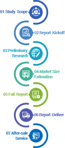
01 Identification of data
This step involves identification of several primary and secondary data research sources, including Global Info Research's internal data sources. The primary sources consist of in-depth discussions and interviews with policy makers, industry experts, and data evaluators, whereas secondary sources include a thorough study of market journals, press releases, annual reports, and government and non-government agencies websites.
-

02 Evaluation of Market Dynamic
This phase includes a detailed evaluation of several factors that are likely to affect the market dynamics. It involves a comprehensive assessment of major market pain points, drivers, and trends. It also comprises a detailed study of research plans and methodology.
-

03 Collection of Data
This process consists of gathering data, accessing proprietary databases, and reaching out to key industry participants that operate in the market across the value chain. It also involves studying several patterns in the historical data and comparing it with the current scenario.
-

04 Collaboration of Data
This stage involves the validation of data and arrival at actual statistics, and evolution of the market over the years. It entails the study and analyzes various segments and verticals of the market. An impact analysis is also performed to observe which factors will affect the market in the next few years.

05 Verification and Analysis
This is the final stage, which involves both quantity and quality checks. Although the process of data verification is an integral part of the research process, all data points and statistics and figures are re-checked to uphold their authenticity and validity.
Companies Mentioned
Hamamatsu Photonics
HORIBA
PLASUS
Extrel
Plasmetrex GmbH
Related Reports


 12 Oct 2021
 Electronics & Semiconductor

Purchase Options

Add To Cart

Buy Now


Popular Product Keywords
- We Provide Professional, Accurate Market Analysis to Help You Stay Ahead of Your Competition.Speak to our analyst >>
Our Clients
What We Can Provide?
With better results and higher quality products,Our professional reports can achieve four things:

Insight into the industry market information

Analyze market development needs

Prospects for future development

Develop industry investment strategy
- Digging deeper into global industry information and providing market strategies.Contact Us >>
